Is A Sheet Of Copper Ohmi

No Freaking Way This Is Brilliant Why Didn T I Ever Think Of That Duh Jewelry Making Tools Jewelry Making Tutorials Creating Jewelry

The Late Hauterivian Faraoni Oceanic Anoxic Event At Rio Argos Southern Spain An Assessment On The Level Of Oxygen Depletion Sciencedirect
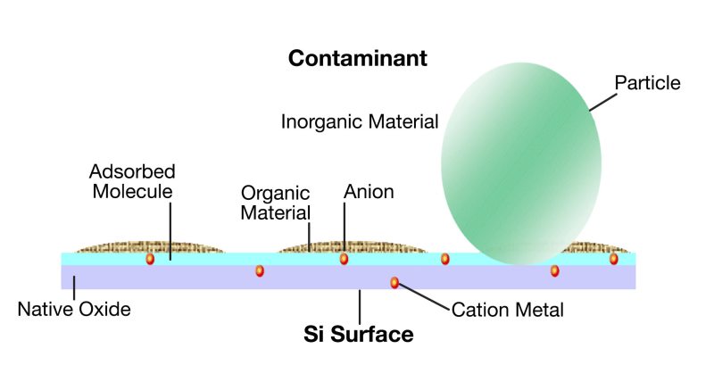
Wafer Surface Cleaning

Materials Free Full Text Luminescence In Sulfides A Rich History And A Bright Future Html
Nanomaterials Free Full Text Supercapacitor Performance Of Nickel Cobalt Sulfide Nanotubes Decorated Using Ni Co Layered Double Hydroxide Nanosheets Grown In Situ On Ni Foam Html
Polysilicon lpcvd in situ.
Is a sheet of copper ohmi.

Valentino Pearly Lace Frame Sunglasses Black Multi 346 Via Polyvore Sunglass Frames Sunglasses Valentino Sunglasses
Https Iopscience Iop Org Article 10 1149 2 0101901jes Pdf

Metal Assisted Chemical Etching Of Silicon A Review Huang 2011 Advanced Materials Wiley Online Library

Detrital Garnet And Chromian Spinel Chemistry Of Permian Clastics In The Renge Area Central Japan Implications For The Paleogeography Of The East Asian Continental Margin Sciencedirect
Source : pinterest.com
